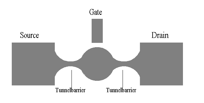
The integration density in microelectronics is progressing in a breath-taking pace despite all predictions about technological and physical limits and will continue at least up to the Gbit generation. But nevertheless pricipal physical limitations are visible. One problem is the power consumption of complex chips. In some cases it has reached values, which cannot be further increased. As the conventional devices and circuits work with large numbers of charge carriers, there should be a great potential for saving energy. E.g. a single bit in DRAM is represented by about 10000 electrons. In contrast, future electronic circuits may handle single electrons, utilizing the so called Coulomb blockade of electron transfer. This effect occurs when the energy to charge a capacitance C by a single electron, e 2 /2C, is larger than the energy of thermal fluctuations kbT, and the tunnel resistance is larger than the resistance quantum h/e 2 . At gate voltages less than e/2C, electron tunneling through the tunnelbarriers onto the island is suppressed and the Coulomb blockade is observed.

Topview of a Single Electron Transistor (after [1])
The benefits of making Single Electron Transistor (SET) memories are the reduced size of the individual memory cells, the reduced power consumption and the possibility to integrate them with Si-logic. A memory cell has only two requirements: 1) that its state can be changed to represent a "1" or "0" and 2) that its state can be sensed. With SET memories this could be accomplished with the movement of a single electron. For today's DRAMs it is done by charging and discharging a capacitor. With SET's the chip of a one terabit memory would not exceed a few cm2. These single electron devices could overcome the limitations of conventional electron devices as dimensions decrease and packing density increases in the future.
In this working group we inverstigate the possibilities of the realization of Single Electron Devices in a thin, highly doped silicon film on top of an insulating oxid [1]. The basic process will start with SOI substrates, involves patterning of a resist layer with hihg resolution electron beam lithography at dimensions down to the 10 nm regime, transfer of the resist pattern by etching into the silicon layer, further reduction of the size of the silicon structure (islands and lateral constrictions that will serve as tunnel barriers) by controlled oxidation down to the 5 nm regime, followed by formation of an overlapping gate.
[1] E. Leobandung, L. Guo and S. Chou, Appl. Phys, Lett. 67, 2338 (1995)